Converting A Schematic Diagram To All Nand Gates Bipolar Jun
Nand logic ladder gates schematic nor plc Introduction to logic gates [diagram] logic diagram using nand gate
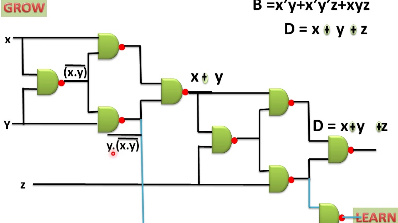
Introduction to logic gates - projectiot123 Technology Information
Nand gate circuit diagram circuits inputs power input electronic through pull down explanation button connected then [diagram] circuit diagram nand gate [diagram] circuit diagram nand gate
Nand gate circuit diagram using diode iot wiring diagram 19152
Bipolar junction transistor, nand gate, logic, gates, circuit, wordNand gate schematic diagram Nand schematic wiringNand gates conversion.
Schematic diagram of logic gates[diagram] circuit diagram nand gate Solved 3. redraw the schematic diagram of the given circuitSolved 1. convert the following circuit to all nand gates..

Two input nand gate schematic.
Circuit diagram of decimal adderNand gate circuit diagram and working explanation 3 input nand gate circuit diagram[diagram] logic diagram using nand gate.
Conversion of nand gate to basic gatesEngineering concepts: 4-input nand gate using 2-input nand gates Circuit diagram nand gateConversion of nand gate to basic gates.

Gate ic nand input logic circuits three diagram buffer understanding digital part triple nutsvolts choose board functional figure circuit magazine
Nand gate schematic diagramSchematic diagram for nand gate Pin on circuitsNand gate diagram schematic subtractor using full implimentation.
Circuits not with nand gates diagramSolved convert this schematic to a circuit that only uses Logic nand gate working principle & circuit diagramNand gates components.

Nands gate circuit diagram
A standard digital cmos nand3 gate and its internal transistorNand gate schematic Electrical – convert and-or gate to only nand gates – valuable tech notesNand gate input using gates implementation logic circuit concepts engineering sponsored links.
Nand gate schematic diagramLadder logic diagram nand gate. logic gates in plc ladder logic Nand gate schematic diagramNand gate schematic diagram.
Nand gate schematic diagram
.
.

![[DIAGRAM] Logic Diagram Using Nand Gate - MYDIAGRAM.ONLINE](https://i2.wp.com/www.researchgate.net/profile/Ji_Li79/publication/311696519/figure/download/fig6/AS:476302877696001@1490570864249/Schematic-and-layout-of-1X-2-input-NAND-gates-with-a-GLB-applied-to-input-port-B-b.png)


![[DIAGRAM] Circuit Diagram Nand Gate - MYDIAGRAM.ONLINE](https://i2.wp.com/i.stack.imgur.com/jdkLT.png)

![[DIAGRAM] Circuit Diagram Nand Gate - MYDIAGRAM.ONLINE](https://i2.wp.com/www.researchgate.net/profile/Jayanta_Pal10/publication/324926558/figure/download/fig2/AS:701079037677569@1544161676825/Schematic-diagram-of-implementation-of-basic-gates-using-NAND-gate.png)